In the semiconductor industry, chip design is a highly complex, cross-disciplinary engineering challenge. As process technologies advance to cutting-edge nodes, a single chip may contain billions of transistors while needing to balance performance, power consumption, area, and reliability. Without powerful software tools, it would be nearly impossible for design teams to complete such enormous tasks within limited timeframes. These indispensable tools are what we know as EDA (Electronic Design Automation) tools.
From Concept to Physical Chip
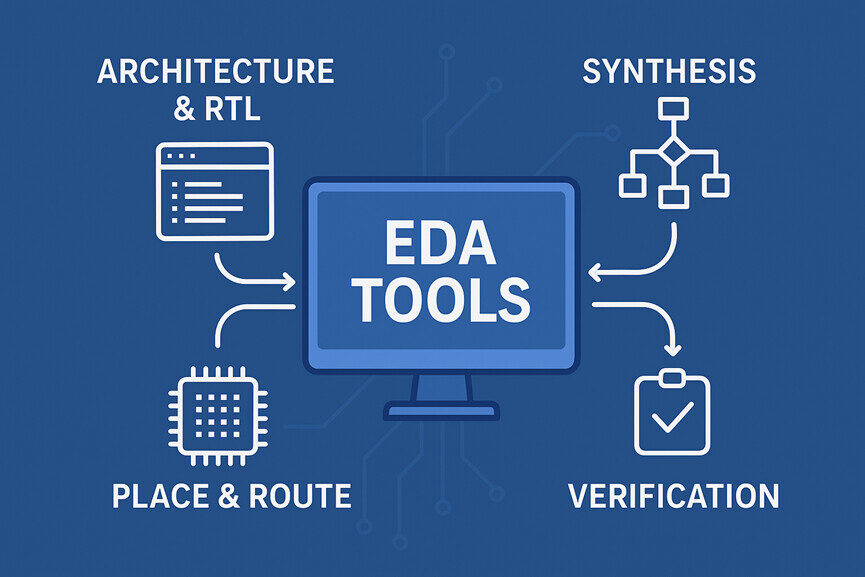
The chip design flow can be broadly divided into front-end design and back-end design. EDA tools span across the entire process, helping designers gradually turn concepts into mass-producible physical products.
- Architecture Design and RTL Coding
At the earliest stage, design teams write RTL (Register Transfer Level) code using hardware description languages such as Verilog, VHDL, or SystemVerilog. EDA tools enable functional simulation at this point to verify whether the logic meets specifications, preventing early design errors from propagating to later stages. - Logic Synthesis
RTL code is converted into a gate-level netlist through synthesis tools, optimized according to constraints such as timing, power, and area. This is a critical step that transforms abstract descriptions into an “implementable circuit.” - Physical Design (Place & Route)
At this stage, EDA tools determine the physical placement of each logic gate and memory block, then complete the routing. As processes scale down, routing density and signal integrity become increasingly challenging, requiring automation tools to handle the massive design scale. - Verification and Sign-off
After layout completion, the chip still needs to undergo timing analysis, power analysis, electromagnetic interference checks, and more. EDA tools help design teams simulate various operating conditions to ensure stability in real-world operation.
Design for Test and Manufacturability
Once chip design is complete, ensuring production yield and reliability becomes another critical step. EDA tools also play an essential role here:
- DFT (Design for Testability): Helps insert scan chains, BIST (Built-In Self-Test), and other test architectures, so that defects can be effectively detected after manufacturing.
- DFM (Design for Manufacturability): Considers process variations and optical effects during layout to ensure that the design can be reliably fabricated by foundries.
These functions not only reduce testing costs but also improve overall chip quality, making them indispensable for high-reliability applications such as automotive and medical electronics.
EDA Challenges in Advanced Applications
As chip applications move toward AI, HPC, and automotive electronics, EDA tools face new challenges:
- Scale Explosion: Chips now contain tens of billions of transistors, making traditional algorithms insufficient. Machine learning and parallel computing are being introduced to improve efficiency.
- Multi-Die Systems (Chiplets): Advanced packaging means system design is no longer limited to a single chip. EDA tools must support integration and verification across dies and packages.
- Functional Safety: In automotive applications, standards such as ISO 26262 require high traceability and safety in chip design, pushing EDA tools to embed corresponding design flow support.
Conclusion
From design to manufacturing, from verification to testing, EDA tools are involved in nearly every step of a chip’s creation. They not only enhance design efficiency but also ensure chip quality and shorten time-to-market. As semiconductor applications continue to expand, the role of EDA will only become more important.
At iSTART-TEK, we continue to invest in this field. Through our proprietary algorithms and testing technologies, we help customers identify potential risks as early as the design and verification stages, enabling the development of high-yield, highly reliable chip products.